Orbit
Projects
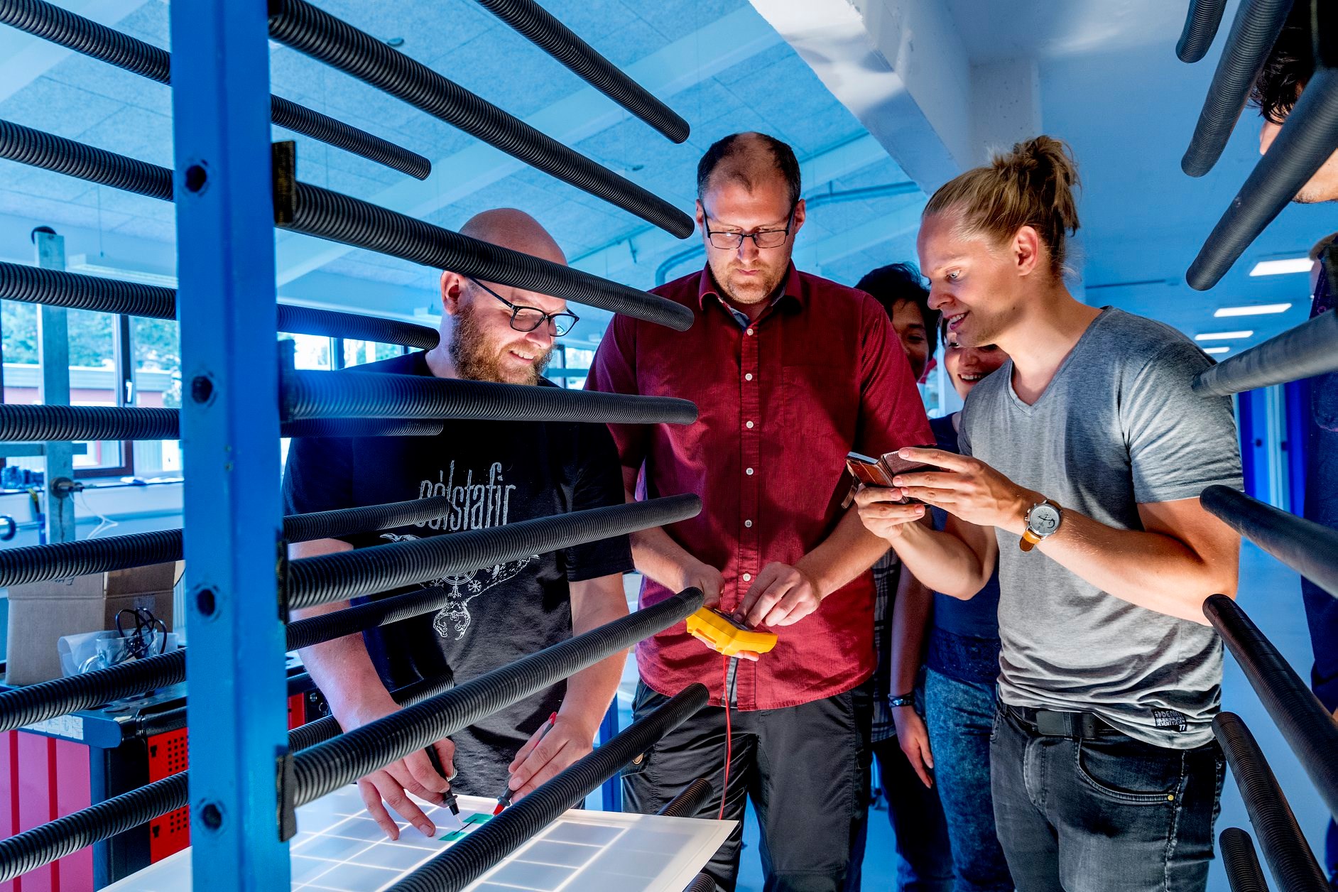
DTU Electro participates in a large number of research projects. Find all projects in our research database.
DTU Electro
Light and electronics - photons and electrons - are the key bits of tomorrows sustainable society. Where they meet, change is made.
At DTU Electro, we combine the immense possibilities of electrical and photonics engineering. Our research is, among other things, used in the healthcare sector for diagnostics, treatment and improving the quality of life. We research into the development of more sustainable energy systems, safer autonomous systems and a faster, greener and more secure internet.

Orbit
DTU Electro participates in a large number of research projects. Find all projects in our research database.
Orbit
DTU Electro is constantly breaking new ground within research.
In our research we strive towards bettering:
At DTU Electro we have a long tradition for industrial collaboration in Denmark and across the borders. We work actively to involve industry partners around a number of research and technology areas.